Major OLED manufacturing supplier Applied Materials has announced what it is calling a breakthrough in OLED display solutions. The new patented technology, called the “MAX OLED solution,” is claimed to not only increase display brightness threefold and increase resolution to around 2,000 PPI, but also reduce power consumption and greatly improve the lifespan of the display. Applied Materials also says that utilizing the MAX OLED solution will allow manufacturers to more easily scale their production, meaning a variety of panel sizes can be produced from a single factory.
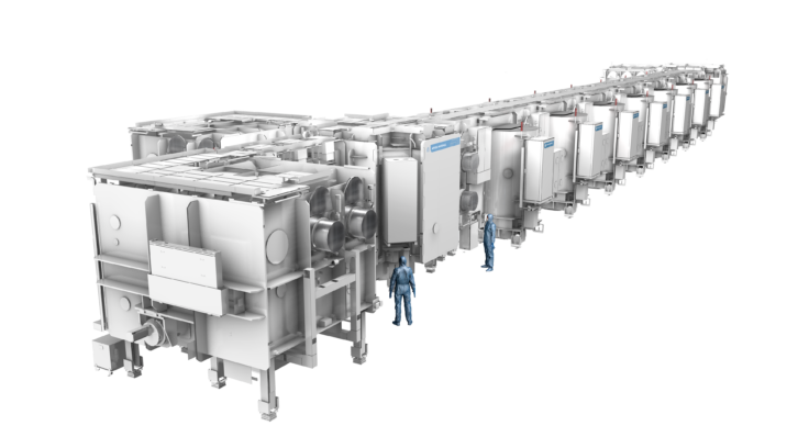
“Applied Materials, Inc. today introduced the MAX OLED solution, a patented OLED pixel architecture and revolutionary display manufacturing technology designed to bring the superior OLED displays found in high-end smartphones to tablets, PCs and eventually TVs,” reads Applied Materials’ announcement. “Applied’s MAX OLED solution makes it easier to scale OLED manufacturing from Gen 6* glass substrates to Gen 8* substrates, which are approximately two times larger, and beyond.”

The company has announced that Samsung Display is one of the launch partners for MAX OLED solution, while industry experts also point to Visionox and Japan Display (JDI) as being first-round adopters of the technology.
See also: TCL highlights its inkjet-printing OLED “breakthrough” at keynote
